- 您现在的位置:买卖IC网 > Sheet目录2007 > MAX11040GUU+T (Maxim Integrated Products)IC ADC 24BIT 4CH 38-TSSOP
MAX11040K/MAX11060
24-/16-Bit, 4-Channel, Simultaneous-Sampling,
Cascadable, Sigma-Delta ADCs
17
Maxim Integrated
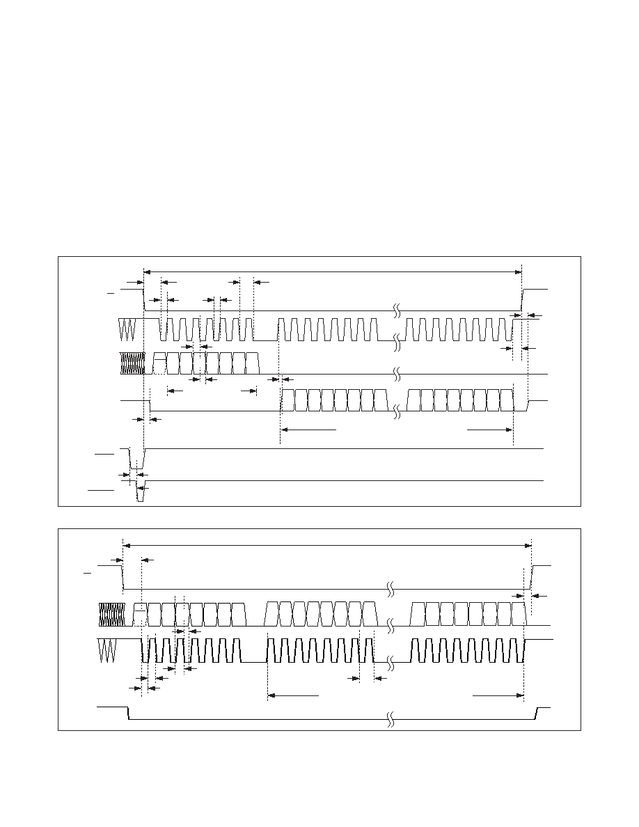
DRDYIN, and DRDYOUT. For single-device applications,
connect CASCIN and DRDYIN to DGND and drive CS
low to transfer data in and out of the devices. With
DRDYIN low, a falling edge at the data-ready signal out-
put (DRDYOUT) indicates that new conversion results
are available for reading in the 96-bit data register. A
falling edge on SCLK clocks in data at DIN. Data at
DOUT changes on the rising edge of SCLK and is valid
on the falling edge of SCLK. DIN and DOUT are trans-
ferred MSB first. Drive CS high to disable the interface
and place DOUT in a high-impedance state.
An interface operation with the devices takes effect on
the last rising edge of SCLK. If CS goes high before the
complete transfer, the write is ignored. Every data
transfer is initiated by the command byte. The com-
mand byte consists of an R/W bit and 7 address bits
(see Table 2.) Figures 7 and 8 show the timing for read
and write operations, respectively.
tCSW
SCLK
CS
DIN
DOUT
DRDYIN
HIGH-Z
B7 B6 B5 B4 B3 B2 B1 B0
tSU
tSCP
tDCD
tCSH1
tSU
tDOE
tDRDY
DATA READY
tHD
COMMAND ADDRESS
tDOT
tPW
R/W A6 A5
A3 A2 A1 A0
A4
DATA LENGTH (NUMBER OF BYTES) DEPENDS
ON THE REGISTER BEING READ (SEE TABLE 2)
DRDYOUT
Figure 7. General Read-Operation Timing Diagram
DOUT
HIGH-Z
tCSW
tSU
tHD
tSU
tPW
tSCP
tPW
tCSH1
CS
DIN
SCLK
A6 A5
A3 A2 A1 A0
B7 B6 B5 B4 B3 B2 B1
R/W
B0
DATA LENGTH (NUMBER OF BYTES) DEPENDS ON
THE REGISTER BEING WRITTEN (SEE TABLE 2)
A4
Figure 8. General Write-Operation Timing Diagram
发布紧急采购,3分钟左右您将得到回复。
相关PDF资料
MAX11046ECB+T
IC ADC 16BIT PAR 250KSPS 64TQFP
MAX11046ETN+T
ADC 16BIT SAMPLING 8CH 56-TQFN
MAX11049ECB+
IC ADC 16BIT PAR 250KSPS 64TQFP
MAX1104EUA+
IC CODEC 8BIT 8-UMAX
MAX11100EUB+
IC ADC 16BIT SRL 200KSPS 10UMAX
MAX11101EUB+
IC ADC 14BIT SRL 200KSPS 10UMAX
MAX11102AUB+
IC ADC 12BIT SPI/SRL 10UMAX-EP
MAX1111CPE+
IC ADC 8BIT LP 16-DIP
相关代理商/技术参数
MAX11040K
制造商:MAXIM 制造商全称:Maxim Integrated Products 功能描述:24-/16-Bit, 4-Channel, Simultaneous-Sampling, Cascadable, Sigma-Delta ADCs
MAX11040K_1111
制造商:MAXIM 制造商全称:Maxim Integrated Products 功能描述:24-/16-Bit, 4-Channel, Simultaneous-Sampling, Cascadable, Sigma-Delta ADCs
MAX11040K_12
制造商:MAXIM 制造商全称:Maxim Integrated Products 功能描述:MAX11040K Evaluation Kit/Daughterboard
MAX11040KDBEVKIT
制造商:MAXIM 制造商全称:Maxim Integrated Products 功能描述:MAX11040K Evaluation Kit/Daughterboard
MAX11040KDBEVKIT#
功能描述:数据转换 IC 开发工具 MAX5135/11040/11612 Eval Kit w/ FMC RoHS:否 制造商:Texas Instruments 产品:Demonstration Kits 类型:ADC 工具用于评估:ADS130E08 接口类型:SPI 工作电源电压:- 6 V to + 6 V
MAX11040KEVKIT
制造商:MAXIM 制造商全称:Maxim Integrated Products 功能描述:MAX11040K Evaluation Kit/Daughterboard
MAX11040KEVKIT#
功能描述:数据转换 IC 开发工具 MAX5135/11040/11612 Eval Kit w/ FMC RoHS:否 制造商:Texas Instruments 产品:Demonstration Kits 类型:ADC 工具用于评估:ADS130E08 接口类型:SPI 工作电源电压:- 6 V to + 6 V
MAX11040KGUU
制造商:MAXIM 制造商全称:Maxim Integrated Products 功能描述:24-/16-Bit, 4-Channel, Simultaneous-Sampling, Cascadable, Sigma-Delta ADCs